Date: November 2011
Duration: 8 weeks
Author: Pablo Manuel Delgado
Description: Phase Locked Loop based effects processor. Original Design.


Sound Sample:
All sounds -except electronic percussion- recorded with a bass guitar through the PLL effects processor. Sample song to show some of the device's capabilities and versatility.
Product Description
The circuit itself is based on a common phase locked loop IC. It utilizes a feedback loop to synchronize an internal oscillator to the fundamental frequency of the input signal, or one of its most prominent harmonics. The oscillator itself acts as a sound wave synthesizer that follows the input signal. The applied input can be any type of signal, i.e. guitar, bass, another synthesizer or line level signal. Its user interface modified parameters are comprised of:
- A Preamp Level: Modifies the preamp level gain in order to provide input signal conditioning for optimal performance.
- A Range control: Modifies the PLL's frequency lock range. The variation of this control provides different synchronization modes of the internal oscillator, changing the processed sound characteristics.
- A Mix knob: Provides a mixing level of the clean and processed signal.
- Volume level
- Envelope Follower switch: A switch that enables a parallel circuit that outputs a rectified control voltage proportional to the input signal level, giving a way of expression dependent of said signal's dynamic range. The control voltage acts over the PLL's range control.
 | |
| PLL Processor's operating scheme. |
Product Design
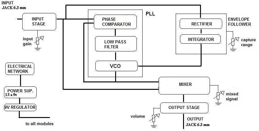
Block Diagram
The next figure represents the device's functional block diagram.
Power Supply
Requirements
Power supply voltage must require sufficient dynamic range to allow full signal excursion and not cause distortion on the signal path. Voltage stabilization is also needed to acquire good oscillator frequency stability.
\begin{equation}
V_{cc} = +9V ± 5\%
\end{equation}
Solution
An integrated LM7809 regulator was used, this IC meets all the required specifications. Due to the good characteristics of the regulator, a simple low power transformer can be used to power the unit fro the electrical network. A voltage range from 9v to 14v is sufficient to accomplish the task, and the regulator will take care of the proper conditioning tasks.
Input Stage
Requirements
Its main purpose is to provide signal conditioning, i.e. impedance matching for the different output Thevenin equivalents that input devices can present. Input signals need also bee independent of musical instruments with passive or active sources, or line level inputs from other sound processing devices/consoles with high output impedances.
\begin{equation}
R_g = 15k\Omega to 100 k\Omega
\end{equation}
A gain control is also needed in order to adapt input signal level to guarantee a good signal tracking.
Solution
A follower configuration was chosen composed of an Operational Amplifier and a serial potentiometer to modify the input impedance and the acquired signal level:
\begin {equation}
R_{in} = 20 k\Omega to 100 k\Omega
\end{equation}
Phase Locked Loop
Requirements
A frequency stability of at least 10% of the input signal's frequency of interest is desired. Also, de capture range must be at least 200 Hz to 10kHz, in order to cover all the possible spectrum characteristics of a fundamental tone of a, say, common musical stringed instrument.
Solution
In terms of the requirements described above and also simplicity and market availability, an integrated solution was proposed for the whole functional block. The CD4046 IC proved sufficient for the desired tasks and specifications. Its main characteristics are:
- Low frequency oscillator thermal stability: 0.04% for each ºC of temperature
- Power supply: 5 to 15V
- Oscillator alinearity: less than 1%
- Capture Range: 10Hz to 1.4Mhz (typical). Controlled by resistive networks.
Envelope Follower
Requirements
The envelope follower is used to change the capture range parameters of the oscillator. This way a modulation of the input signal is provided depending on the input signal's voltage swing. The main purpose of this inclusion is to provide a mean of expressiveness coming from the instrument that is going to be processed. The envelope follower circuit itself is comprised of a rectifying circuit and an integrator, its time constant was calculated to provide minimum ripple on lower frequencies and to provide a good rectified control signal.
Solution
The topology chosen for the envelope follower is shown below.
 | |
| Envelope Follower with optical coupling |
The coupling mode for the control range input of the CD4046 is an optical one. The chosen optocoupler was HF113 FET (optical varying resistor) and it provides the desired transfer characteristics to generate a good control signal based on varying resistance of the equivalent control network applied to the PLL. A current calibration potentiometer is also included, as well as a manual switch that passivises the follower circuit. The resistors were calculated as to have a maximum voltage transfer, as well as a suitable control current for the HF113. The integrator's time constant was approximated by simulation and finally determined in practice:
\begin{equation}
Time = \frac{RC}{2.2} = 2.2 \times 1 \mu F \times 100 k \Omega = 0,22 seg.
\end{equation}
Mixer and Output Stage
Requirements
The output stage must be in charge of providing a correct output impedance for interconnection with other sound processing units, consoles or amplifiers.
\begin{equation}
R_{out} = 100k \Omega
\end{equation}
it is also needed to provide a volume control stage.
Solution
A follower configuration is employed with an operational amplifier and an output potentiometer to implement the volume control. A similar configuration is used to adapt both signals, processed and unprocessed, which paths converge to a linear potentiometer with three terminals,i.e. the mixer control.
Other considerations
Sound Quality
The figure of merit perceived by potential clients as "sound quality" can be translated into a series of quantifiable parameters:
- Noise immunity performance
- Line interference rejection (i.e. 50 or 60Hz) and humming
- Low interstage distiortion
- A sufficient dynamic range of operation in order to avoid signal saturation and unwanted peaks
- Bootstraping of the unprocessed signal, i.e. maintain the unprocessed signal as clean as possible
The operational amplifiers chosen (TL072) resulted in a critical component on the test bench, due to its good noise immunity and signal performance. The dynamic range is that of 0V to 9V with an operating bias point of 4.5V for symmetry.
The coupling capacitors are electrolytic and ceramic ones of low tolerance. These are commonly used on the industry as this equipments does not pretend to be a high fidelity audio amplification unit.
Schematic Diagram

PCB Layout
 | |
| PCB Layout and component distribution |

Polarity inversion protection circuit
The most important element at the time of determining the failure rate was the LM7809 to provide stability for the oscillator. This regulator provides low failure rates given that accidental polarity inversion is not produced. An improper borne connection or transformer polarity could cause overheating, destroying the regulator's circuits in just a few seconds.
A simple diode voltage inversion protection was implemented
 | |
| Polarity inversion circuit |


No hay comentarios:
Publicar un comentario